How to 3D Print a Solder Paste Stencil
A step-by-step guide to creating precise SMD stencils from your Gerber files using an FDM 3D printer
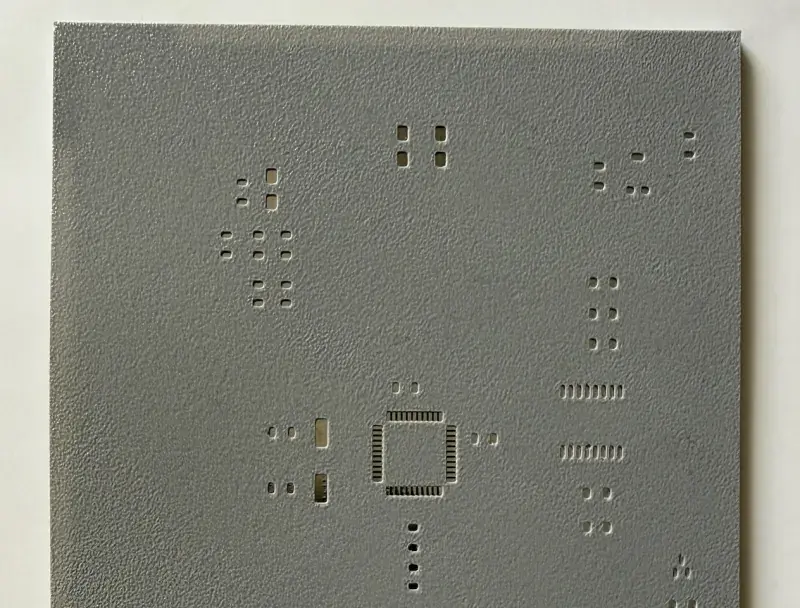
A 3D-printed solder paste stencil, ready to use on a PCB.
What is a Solder Paste Stencil?
A solder paste stencil is a thin plate with cutouts that match the solder pads on your PCB. You place it over the board, spread solder paste with a squeegee, and the paste is deposited precisely on each pad.
Stencils are essential for SMD/SMT reflow soldering. They make the process faster and more consistent than applying paste by hand with a syringe.
3D Printed vs Professional Stencils
3D-printed stencils are a low-cost alternative ideal for prototyping and small batches. For final production boards with fine-pitch components, professional laser-cut stencils remain the reference.
| 3D Printed (Stenchill) | Professional (laser-cut) | |
|---|---|---|
| Cost | Free (just filament) | $15-30 per side |
| Turnaround | Minutes | Days (shipping) |
| Precision | Good (0.2-0.4mm nozzle) | Excellent (laser-cut) |
| Best for | Prototyping, small batches, 0603+ components | Fine-pitch QFN/BGA, production runs |
Close pads: what to do?
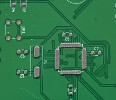
On fine-pitch footprints like QFN, QFP or SOIC, pads can sit so close together that the walls between them are too thin to print reliably. If you leave Merge close pads on (the default), I fuse each row into a single slot. If you turn it off, I stay true to the original layout and trust your slicer.
Don't want paste on every pad?
A part you won't fit
A board variant, an optional footprint, a spot left empty for now.
A connector you hand-solder
It goes on with the iron after reflow, so it needs no paste.
A stray alignment mark
Some EDA tools put fiducials on the paste layer, and they end up punched in the stencil.
Your file
Connector removed
After generating, open Remove pads under the 3D view. Click the pads you don't want, or drag a rectangle around an area, then hit Regenerate.
I rebuild the whole stencil as if those pads had never been in your Gerber, so the pads around them are recomputed too. Restore all puts everything back.
What You Need
- Gerber files from your EDA tool (KiCad, Eagle, Altium, or any other)
- An FDM 3D printer (any standard model works)
- PLA or PETG filament
- Solder paste and a squeegee
- Stenchill (this website) or the KiCad plugin
Step-by-Step Guide
Export your Gerber files
In KiCad, go to File → Plot, select Gerber format, and make sure the Paste layers (F.Paste, B.Paste) and Edge.Cuts are included. In Eagle or Altium, use the standard Gerber export. You need at least a Paste layer and the board outline.
Upload to Stenchill
Go to the Stenchill homepage, drag and drop your Gerber ZIP file, or use the individual files mode to select only the layers you need. You can also use the KiCad plugin to generate directly from the PCB Editor.
Adjust settings
Configure the generation parameters: stencil thickness (0.3-0.4mm recommended for most components), shrink value, nozzle diameter for automatic compensation of small pads, and shoulder options for PCB alignment.
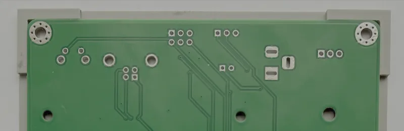
The registration supports hold the stencil perfectly aligned on the PCB. They are generated automatically from the board outline.
Download and slice
Download the generated STL or 3MF file. In your slicer, use these settings: 0.1mm layer height, 100% infill, 3-4 layers total (matching your stencil thickness). A 0.2mm nozzle gives the best results, but 0.4mm works too with nozzle compensation enabled.
Slow your print speed to 30 - 40 mm/s. Stencils are tiny, fine-detailed prints, and slower toolhead movement gives the extruder time to lay down clean pad edges instead of skipping fine features.
If your slicer supports it (Cura, PrusaSlicer, OrcaSlicer, BambuStudio), switch the Wall generator from Classic to Arachne. Arachne adapts wall widths to the exact opening geometry and avoids the tiny gaps that Classic can leave on pads narrower than the nozzle. If your slicer only has Classic (older Slic3r derivatives, basic slicers), the stencil still prints - just with slightly less precision on the finest pads.
Print on a smooth bed surface (glass, smooth PEI, mirror). Because the face touching the bed mirrors its texture, a smooth bed gives you a perfectly flat side to spread solder paste across, and the squeegee glides without catching. Textured beds (textured PEI, granular surfaces) still work, but the imprinted bumps make paste harder to spread evenly.
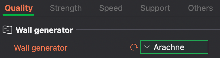
In BambuStudio (shown), set Quality → Wall generator to Arachne before exporting G-code. Cura, PrusaSlicer and OrcaSlicer expose the same option.
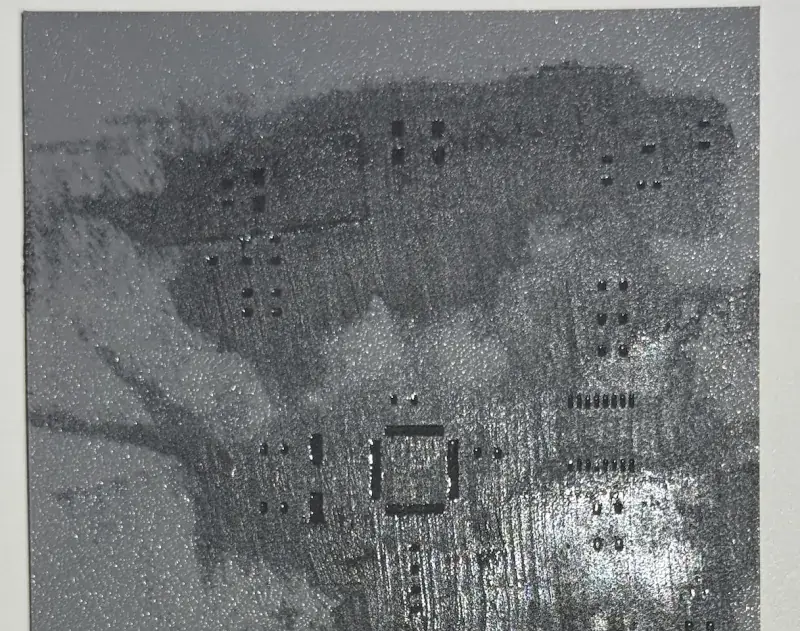
Spread solder paste with a squeegee across the stencil openings, then carefully lift the stencil off the PCB.
Apply solder paste and reflow
Place the stencil on your PCB. The registration shoulders automatically align it. Spread solder paste across the openings with a squeegee. Remove the stencil carefully, place your SMD components, and reflow using a hot plate, reflow oven, or hot air station.
Tune the paste volume with thickness
I derive the opening area from your paste layer, so thickness is the one term you control. Starved joints? Go up to 0.5 mm. Paste bridging between pads? Go down to 0.3 mm.
Reach for thickness before shrink. Shrink reshapes every opening, so it changes where paste lands; thickness scales the volume and leaves the layout alone.
Keep the value a multiple of your layer height, or the slicer rounds it for you. At 0.1 mm layers, 0.3 / 0.4 / 0.5 mm print exactly.
Which nozzle does your board need?
Your components' pitch decides your nozzle, not the other way round. Between two neighbouring openings I need a wall at least one nozzle wide for the printer to render it, and each opening at least two nozzles wide for the paste to release. So the distance from one pad centre to the next has to be at least three times your nozzle diameter.
An 0805 or a SOIC at 1.27 mm pitch prints fine with a 0.4 mm nozzle. A 0.65 mm QFP wants 0.2. A 0.5 mm QFN or BGA wants 0.15, and a 0.4 mm BGA wants 0.1, which is about the finest you can readily buy.
Your nozzle also sets the shoulder clearance
A finer nozzle does not mean a tighter fit. The clearance is applied on each side of the board, so the real play is double the value you type, and below roughly 0.20 mm the stencil no longer slides between the shoulders. Stenchill suggests the value below as you change the nozzle, and warns you when yours is far from it.
Measured on one printer, so treat it as a starting point rather than a law. If the stencil goes in tight, add one step of 0.05 mm: too loose only costs a little alignment accuracy, too tight costs the whole print.
Tips & Troubleshooting
Paste bleeds under the stencil
Check that the stencil sits flat on the PCB. Use tape or clamps to hold it in place. Make sure the bottom surface is smooth (print on a glass bed).
Small pads don't print correctly
Use a 0.2mm nozzle for best results with fine-pitch components. If using a 0.4mm nozzle, enable nozzle compensation in Stenchill. It automatically enlarges pads that are too small for your nozzle.
Stencil warps after printing
Print on a heated glass bed for best flatness. PETG warps less than PLA. Make sure your first layer adhesion is good and avoid removing the stencil while it's still warm.
Shoulders don't fit the PCB
Increase the clearance parameter in the settings. The default 0.3mm works for most PCBs, but if your board is slightly oversized, try 0.5mm.
Pads printed partially filled or skipped
If your slicer supports it (Cura, PrusaSlicer, OrcaSlicer, BambuStudio), switch the wall generator to Arachne. It produces variable-width walls that fit narrow pad openings, whereas the Classic generator skips or under-fills walls thinner than the nozzle.
Bambu Studio says the 3MF has an invalid config
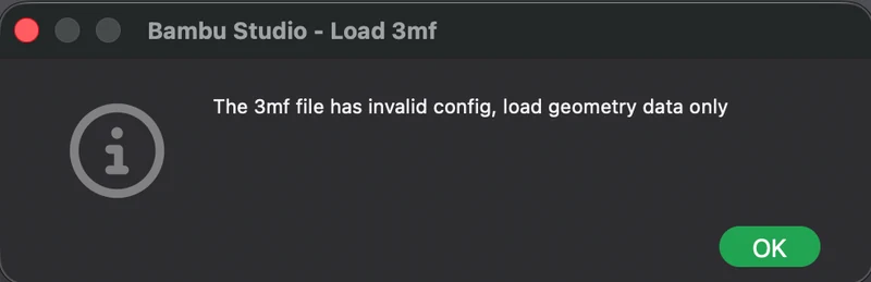
Click OK, the file is fine. Bambu Studio only reads print settings out of 3MF files it wrote itself, so it reports every other 3MF as having no config and loads the geometry on its own. That is what you want here: the stencil arrives whole, at the right scale, and your own print profile stays selected. OrcaSlicer shows a similar notice. If you would rather not see it, slice the STL instead, it carries the same stencil.
Ready to try?
Generate your stencil in seconds. It's free, no account required.